Transport at Nanoscale Interfaces Laboratory
Education
Lectures (University of Basel, ETH Zürich)
A list of our current and past lectures is available here.
PhD students
University of Basel: Doctoral studies | Semesters Dates and deadlines | Documents and regulations.
Master Projects
Our lab offers a variety of Master projects for students. For more details visit our masterproject-section and do not hesitate to contact the responsible persons.
Lehrstelle: Physiklaborant/-in
Jedes Jahr bilden wir Physiklaborant/-in EFZ aus. Wenn dich diese vielfältige Ausbildung interessiert, bewirb dich rechtzeitig auf diese Stelle! ;-)
IAESTE students
Our Lab regularly offers opportunities for IAESTE internships.
TimeTrace.jpg
Version 1.0 Approved
- Document Type
- Basic Document
- Extension
- jpg
- Size
- 25 KB
- Modified
- 11/4/25 8:40 AM by Ivan Shorubalko
- Created
- 11/4/25 8:40 AM by Ivan Shorubalko
- Expiration Date
- Never Expire
- Review Date
- Never Review
- Location
- Nanoelectronics and Nano-Optics
-
Version 1.0By Ivan Shorubalko, on 11/4/25 8:40 AMNo Change Log
Graphene - Quantum Dot Photodetectors

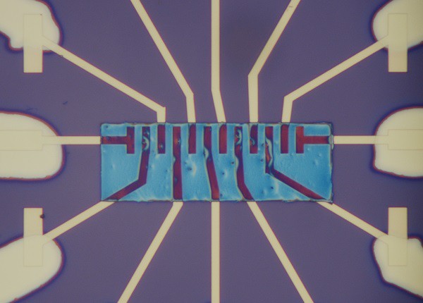
Combining high mobility graphene transistors with efficient light absorbing colloidal quantum dots may pave a way for cheap, high resolving infrared photodetectors. Light is absorbed in the Quantum Dot layer, creating excitons. One charge carrier type is transferred faster to the biased graphene transistor, leading to an additional electric field. This is measured by a current change in the graphene transistor. We are investigating the detailed mechanism of these graphene-QDs photodetectors, expanding the range of spectral photoresponse, increasing the detectivity, and scalling down to the device size below the light wavelength.
Further sources:
Master projects
Our lab offers a variety of Master projects for students.
For more details do not hesitate to contact responsible persons.
| Title | Contact person(-s) |
|---|---|
| THz Boradband Metalenses | Elana Mavrona |
| Time Resolved Photoluminescence Spectroscopy and Simulations | Mirjana Dimitrievska |
| Charge and heat transport through graphene nanoribbon based devices | Mickael Perrin |
| Decoding Alzheimer’s Protein Aggregation in Body Fluids | Peter Nirmalraj |
| Machine Learning Augmented Red Blood Cell Imaging and Analytics | Peter Nirmalraj |


