Coatings and Miniature Mechanics
The group focuses on the designing methods and instruments to assess mechanical properties and reliability of miniature systems and coatings, as well as investigating the mechanical behavior and failure mechanisms of such components. The challenge of such task relay on the non-uniformity microstructure of deposited parts, the presence of interfaces and residual stress in the systems as well as the lack of available methods to extract material properties under complex load cases (fatigue, multiaxial loading).
Measurement of fatigue process in thin films

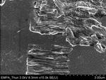
Thin films are an important part of modern technology. They are used in chips, screens and as protective or functional layers. With the increase of use, the need to improve lifetime also comes into focus of research. The lab for materials- and nano mechanics investigates the fatigue process of thin films (from 100 nm to 2 um in thickness) in order to improve their lifetime. Thin films are coated on silicon beams, which oscillate at their resonance frequency, in order to cause fatigue in the films by cyclic bending of the cantilevers. The advantage of this setup is the linear strain distribution along the cantilever, which allows the observation of fatigue depending on the strain amplitude. The progress of fatigue is observed by EBSD, SEM and BSE measurements. With these techniques it is possible to observe and investigate the dif-ferent mechanisms involved in plastic fatigue. Of special interest is the influence of the film’s microstructure and thickness on the fatigue life time.
Micro-scratching/machining
This motivated our interest to investigate the deformation mechanisms as a function of grain orienta-tion by means of in-situ microscratching experiments in combination with electron back scattered diffraction technique (EBSD). Through this study it could be shown that crystal orientation affects the de-formation behavior, as activated slip systems change their orientation with respect to the sample surface and plastic deformation is propagating into different directions. Thus, it is possible to improve the micro-machinability of crystalline materials if the crystal orientation is known with respect to the machining direction so that preferred directions favoring chip formation over pile-up could be selected, resulting in better surface finish and lower forces during the cutting process. For textured materials, this finding might be even applicable on a larger scale.

-
Share
