Functional Thin Film Solution Processing
|
|
 |
|
Exciton dynamics and effects of structural order in morphology-controlled J-aggregate assemblies. |
Two‐dimensional transition metal carbides |
|
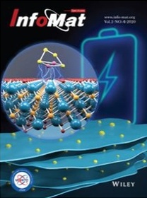
Two‐dimensional MXenes for lithium‐sulfur batteries. |
A Universal Approach for Room-Temperature Printing and Coating of |
Thanks to advances in materials chemistry, researchers have been able to synthesize new materials that allow solution-based processing of next-generation optoelectronic materials
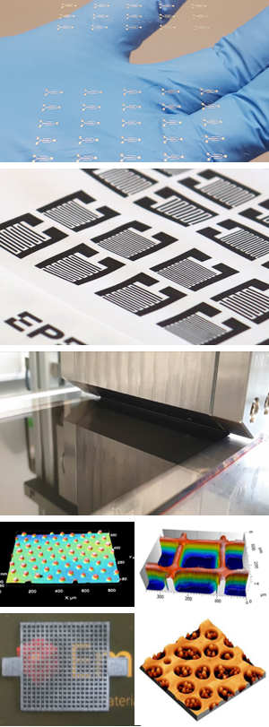
In Printed Electronics, printing technologies are used to produce various kinds of devices, such as electronic circuits, sensors and solar cells. New challenges arise when small scale laboratory processes are transferred to industrially relevant methods.
In the “Functional Thin Film Solution Processing” group, we address scientific and engineering aspects of solution processing, namely
- to overcome the gap between lab-scale sample manufacturing and industrially relevant fabrication technologies. We improve gravure printing as manufacturing technology for printed electronics and slot die coating for up-scaling perovskite solar cell manufacturing.
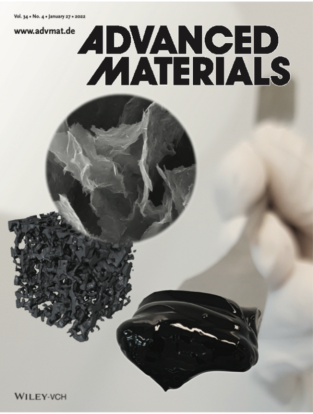
- to develop novel ink formulations from 2D materials.
- to exploit spontaneous self-assembly related to solvent evaporation to add functionality to wet deposited films.
Our coating laboratory provides infrastructure, workforce and knowhow for the deposition of functional coatings and protection layers on rigid and flexible substrates used for the fabrication of optical and electronic devices.
Available equipment at the coating laboratory will enable the development of thin film coating solutions up to DIN A5 scale. The laboratory will evaluate, develop and offer the best-suited technology and analytic for a given functional coating.
Recent publications:
S. Deng et al., Multifunctional SnO2 QDs/MXene Heterostructures as Laminar Interlayers for Improved Polysulfide Conversion and Lithium Plating Behavior. Nano-Micro Letters, 2024, 16, 229. https://doi.org/10.1007/s40820-024-01446-w
I. Brunetti et al., Fully Screen-Printed, Flexible, and Scalable Organic Monolithic Thermoelectric Genera-tors. Advanced Materials Technologies, 2024, 9(11), 2302058. https://doi.org/10.1002/admt.202302058
V. Vlnieska et al., Polypy: A Framework to Inter-pret Polymer Properties from Mass Spectroscopy Data. Polymers, 2024, 16(13), 1771.
https://doi.org/10.3390/polym16131771
S. Abdolhosseinzadeh et al., MXene Inks for High-Throughput Printing of Electronics. Advanced Electronic Materials, 2024, 2400170.
https://doi.org/10.1002/aelm.202400170
C. (J.) Zhang et al., Micro‐Cup Ar-chitecture for Printing and Coating Asymmetric 2d‐Material‐Based Solid‐State Supercapacitors. Small. 2023, 19(32), 2300357. https://doi.org/10.1002/smll.202300357
Dr. Jakob Heier
Phone: +41 58 765 4356
jakob.heier@empa.ch
NEWS
2024
February:
We welcome Rossella Galli to our group. Rossella is a exchange PhD student and will stay for 4 months.
March:
We congratulate Junjie Cai on completing her master's degree.
Mai:
We welcome Tobias Kuster to our group. Tobias is doing his Civil Service on the topic "Effiziente umweltfreundliche Solarenergie".
FUNDING

