Focused Ion Beam systems at Empa

FIB - a microscope turns into a workbench

Jul 22, 2002 | BEAT ASCHWANDEN

Until recently the two FIB (Focused Ion Beam) systems at Empa were only used for fault analysis and the modification of modern microchips and semiconductor devices. Now, however, they are also being successfully applied to solve problems in material science, surface and joining technology, and biology.

/documents/56164/322739/a592-2002-06-24-01-b1m+FIB-Einweihung.jpg/f16ea9e0-e2a0-4773-8ab5-49701f0f7aa4?version=1.0&t=1448309284046
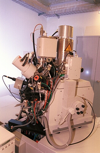
One of Empa's FIB systems
 

Microcircuit design errors

Because of the extremely complicated manufacturing processes involved in producing microchips, any errors in the circuit design have very serious effects on development and delivery times. Correcting faults using classical process lithography can take several weeks, and only then does the Design Engineer know whether or not his chip functions at all.

 
137 KB
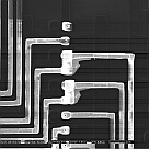
Modifications being made to a microchip.
 

FIBs offer an alternative which is faster and usually more economic: repairing the chip with an ion microscope (whose resolution and magnification are orders of magnitude better than an optical microscope) takes perhaps a few hours.


The two FIBs, which are located in a laboratory of the Electronics/Metrology Section, function as follows: a flow of suitable gases is directed onto the fault, which is also exposed to a beam of gallium ions. With an accuracy of a tenth of a micrometer, localized "micro-reactions" are produced. Depending on the operating conditions, thin electrically conductive layers of tungsten or platinum, or insulating layers of silicon oxide are deposited with extreme spatial precision. With its ability not only to deposit material but also make cuts into the sample, FIBs find applications beyond mere microscopy and have become a sort of workbench for repairing faulty micro-structure prototypes. This has extended the scale of Empa's range of operating and research activities from daringly innovative road-bridge construction to the characterization of tiny structures just a few nanometers in length.


182 KB
Beneath damaged surfaces more is concealed...
 

New applications for the FIBs at Empa

FIB methods have established themselves in fault analysis and the modification of modern microchips and micro-mechanical systems (MEMS – Micro Electric Mechanical Systems, and MOEMS – Micro Opto-Electric Mechanical Systems) over the past few years. However in other scientific fields with similar requirements, such as material science, surface and joining technology, and biology, this technique is hardly known.


With its two FIB systems, conceived to encourage interdisciplinary activity, Empa is creating a link between conventional and newly discovered areas of application.


A case for the FIB in surface technology

An example of damage analysis demonstrates how useful a FIB can be to surface scientists. In the case in question the FIB was being used to inspect a seemingly minor fault in the paint on a car door. The fault was barely visible with a magnifying glass, but the FIB micro-profile exposed an unexpected and serious problem. The side view of the sample, also taken "in situ" by the FIB, clearly showed how an air inclusion in the primer layer had gradually expanded into the paint layers above to form a large bubble. The result was a huge hollow space directly under the paint surface which was practically invisible externally. The potential for later damage by corrosion due to the effects of trapped salt water was enormous.


162 KB
The FIB is located in a vibration-isolated cellar.
 

What is an FIB?

The basic principle of the FIB is simple: a normal scanning electron microscope (SEM) is used, but the electron source is replaced by a gallium ion gun. The electrons emitted by the source in a REM strike the atoms in the sample, knocking electrons out of them but without significantly altering them.


These secondary electrons, as they are called, give information about the topography and material characteristics at the point where the (primary) electron beam strikes the sample surface. The primary electron beam is scanned point by point and line by line over the sample, as in a television picture, giving a detailed and greatly magnified image.

The advantage of the FIB over the SEM lies in the fact it uses a gallium ion beam, and gallium ions are orders of magnitude heavier than electrons, so that the interaction of the ion beam with the sample is much more pronounced. If the electron beam were likened to the beam of a torch, then the ion beam would be comparable to a very powerful but finely controllable laser beam. The laser beam, to continue the analogy, causes material from very precisely targeted points on the surface of the sample to be knocked out, a process called sputtering. This is exactly what happens in the FIB, on an incredibly small scale. A by-product of the bombardment with gallium ions is, of course, secondary electrons which are also ejected. These allow an image of the sample to be generated (in addition to the other FIB operations on the sample) which is of similar quality to that produced by a good SEM.

The «dernier cri» of FIB technology is the combination of FIB, gas chemistry and classical SEM in one machine. This set-up is known as Dual-Beam FIB, and multiplies the advantages of the FIB with those of classical scanning electron microscopy. The Dual-Beam FIB technique has advantages in certain applications, such as the rapid and precise preparation of samples for transmission electron microscopy (TEM). While TEM is capable of even greater magnification than SEM, sample preparation was traditionally a specialization mastered by very few experts in the field. One of the two systems at Empa is a Dual-Beam FIB.


Links

Medienmitteilung FIB-Einweihung: 407 KB (in german available only)