Transport at Nanoscale Interfaces Laboratory

Dec. 07, 2020 Lab 405 image contest

Our laboratory had this fall 2020 for the first time an internal image contest with multiple contributions.

...and the winners are...

Gökhan, Lars & Roman. Congratulations!!

Their pictures enclosed:

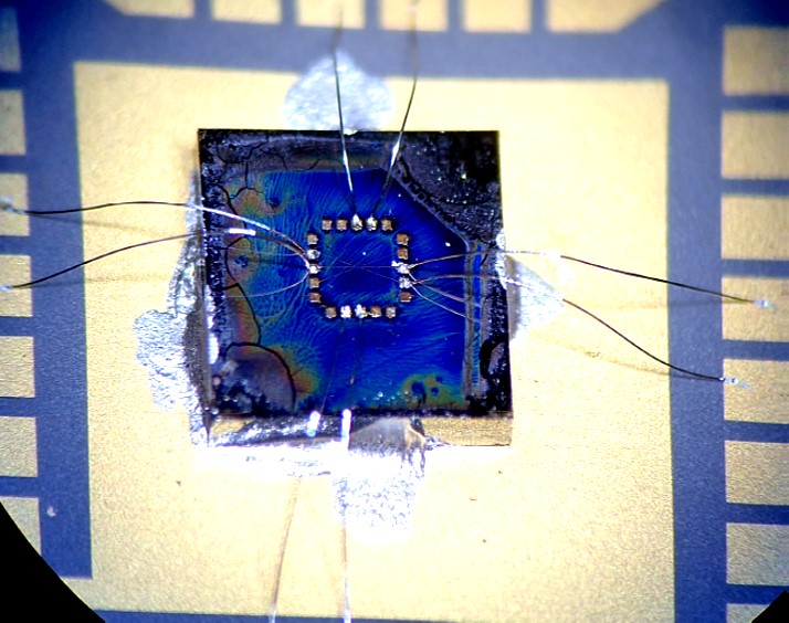
Gökhan Kara: The image shows graphene – PbS QDs phototransistors contacted to a chip carrier. The spin-coated 200 nm QDs film can be seen in blue.


Lars Lüder: A chemiresistive sensor device detects target analytes based on an electrically conductive metal-organic framework (MOF). When entering the MOF-pores, the analytes interact with the MOF which increases the resistance by limiting the charge transport.


Roman Furrer: Graphene – Where worlds collide and beauty appears at small scale! The image shows not full coverage grown CVD graphene, transferred on Silicone Oxide. The orientation of the graphene "crystals" depends on the underlying copper grain.