
Low Dimensional Materials
Our group is developing novel low dimensional nanostructures & nanomaterials using combinations of state of the art deposition techniques: molecular layer deposition (MLD), atomic layer deposition (ALD), physical vapour deposition (PVD), and local focused electron and ion beam induced chemical vapour deposition (FEBID, FIBID).
Our R&D activities are driven by finding novel nanostructured materials for sustainable energy technology, nanotechnology, and health issues. Special focus is given to the development of:
i) Surface functionalization of non-planar substrate architectures:
developing MLD and ALD for conformal coatings of highaspect ratio, open porosity, non-planar substrate architectures, like nanowire and nanotube carpets, perforated membranes, andhigh surface assemblies in energy storage or production assemblies.
ii) Novel low dimensional model materials
iii) Non-conventional 3D nanoprinting for device prototypes:
iv) Theoretical frameworks for materials design and enabling synthesis control:
Molecular and Atomic Layer Deposition in high-aspect ratio architectures
MLD and ALD are rely on self-limiting surface reactions of sequentially supplied differing volatile molecules enabling uniform and homogeneous film growth without clogging the surface of open surface porosity material at comparatively low growth temperatures. Among the films and multilayers we investigate figure TiO2, Al2O3, ZnO, Y2O3, Al(Eg), and Al(Gl) materials. Substrates we use range from polymers to metals and semiconductors as well as more sophisticated architectures as nanotube arrays, porous aggregates for battery applications, and natural materials like cellulose and wood.
Book Chapter: C. Guerra, H. G. Park, I. Utke, ALD for interface engineering in: Atomic layer deposition in energy conversion applications. J. Bachmann, Wiley-VCH, 2017.
C. Guerra-Nunez et al., Reaction and Growth Mechanisms in Al2O3 deposited via Atomic Layer Deposition: Elucidating the Hydrogen Source, Chemistry of Materials, doi: 10.1021/acs.chemmater.7b02759, 2017.
Y. Zhang et al., Atomic Layer Deposition of Titanium Oxide on Single-Layer Graphene: An Atomic-Scale Study toward Understanding Nucleation and Growth, Chemistry of Materials. doi I: 10.1021/acs.chemmater.6b05143, 2017
C. Guerra et al., Morphology and Crystallinity Control of Ultrathin TiO2 Layers deposited on Carbon Nanotubes by Temperature-Step Atomic Layer Deposition, doi: 10.1039/c5nr02106e, 2015.
Minimally invasive 3D nanoprinting with local focused electron and ion beam induced chemistry
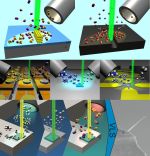
Gas assisted Focused Electron/Ion Beam Induced Processing (also known under the acronyms FEBIP and FIBIP) constitutes a non-conventional rapid 3D nanoprinting platform which allows for synthesis (deposition and etching) of conventional and novel materials for nanodevices. We investigate a) the underlying key physico-chemical processes to gain compositional and shape control over the process, b) the synthesized novel granular and nano-composite material with respect to electrical, magnetical, mechanical, and optical properties using specifically developed SEM-integrated measurement setups, c) develop nanodevice prototypes, like magnetic bead sensors, polarization gratings for telecom lasers, and tip en-hanced Raman spectroscopy.
K. Hoeflich, Katja et al., Towards the third dimension in direct electron beam writing of silver, doi:10.3762/bjnano.9.782018, 2018.
K. Hoeflich et al., Direct Electron Beam Writing of Silver-Based Nanostructures, doi: 10.1021/acsami.7b04353, 2017.
M. V. Puydinger dos Santos et al. Annealing-Based Electrical Tuning of Cobalt−Carbon De-posits Grown by Focused-Electron-Beam-Induced Deposition, doi: 10.1021/acsami.6b12192, 2016.
Book chapter: I. Shorubalko, Lex Pillatsch, and I. Utke, Patterning & Deposition with noble gases, pages: 355-388, in: Helium Ion Microscopy, Editors G. Hlawacek, A. Gölzhäuser, Springer DOI 10.1007/978-3-319-41990-9, 2016.
Highlight: I. Utke and A. Goelzhaeuser, Small, Minimally Invasive, Direct: Electrons Induce Local Reactions of Adsorbed Functional Molecules on the Nanoscale, Angew. Chem. Intl. Ed. 49(49) (2010) 9328, DOI: 10.1002/anie.201002677.
Theory Frameworks
Simulations and models are vital for optimization of process and materials parameters. We develop continuum as well Monte Carlo approaches to cover different length scales in our experiments. Freeware (source codes and executable) simulators are available on this website FEBID CODES LINK for rarefied molecule flow and growth by focused electron beams.
Related papers:
W. Szmyt et al., Diffusion of dilute gas in arrays of randomly distributed, vertically aligned, high-aspect-ratio cylinders, doi: 10.3762/bjnano.8.7, 2017.
M. Toth et al., Continuum models of focused electron beam induced processing, Beilstein Journal of Nanotechnology 6, 1518-1540, doi:10.3762/bjnano.6.157, 2015.
V. Friedli and I. Utke, Optimized molecule supply from nozzle-based gas injection systems for focused electron- and ion-beam induced deposition and etching: simulation and experiment. J. Phys. D: Appl. Phys. 42 (2009) 125305, doi:10.1088/0022-3727/42/12/125305.
Equipment/Service
All equipment is available for prototyping within joint fundamental research or industrial research projects.
Stationary ALD/MLD reactor: lab-built reactor allowing for 4 inch wafers, Full control over temperature and variable cycle/purge/exposure periods as function of total cycle number.
Benchtop Arradiance reactor: with vapour push through feature for low volatility precursors and QCM for in-situ growth control. Also features glove box connection for air sensitive samples.
PVD ALD/MLD cluster reactors: Mantis PVD chamber has two DC and one RF magnetron sputter unit, one e-beam evaporator, and one nanoparticle gun. In-vacuo shuttle to ALD/MLD reactor with multilayer automated option.
Mobile ALD/MLD setup: viscous flow or stationary mode with varying reactors (mini-reactors for in-situ Raman studies, flow through reactor for membranes).
PVD Mantis: 1e-8 mbar vacuum with two DC magnetron sputter sources and one RF source, mini-ebeam evaporator with 4 independent sources, and one nanoparticle gun.
SEM Hitachi S3600N (tungsten electron emitter) with XENOS lithography,heatable gas injec-tion systems, heatable substrate stages, and nanomanipulation: Dedicated variable pressure SEM for FEBIP chemistry development and classical e-beam lithography.
FIBSEM, Tescan Vela (W-emitter, Ga-ion source) with lithography and gas injection, nan-manipulation: for FIBIP, ion milling, FEBIP.
FIBSEM, Tescan Lyra3 (FEG, Ga-ion source) with e-beam/ion lithography and gas injection system, FIBSIMS.
Residual Gas Analyser: Stanford Research System 300AMU.
RF Plasma Cleaning system, XEI: Evactron 24/25.
More SEM integrated setups: 4-point probing station with 15 translational axes, compres-sion/indentation setups (10 mN, 1mN), three translational axes nanomanipula-tion/nanopositioning systems, superparamagnetic bead detection system, AFM in SEM, vibra-tional table.
