
Process for manufacturing nanoelectronic “mini-circuits” developed
Nanowires for the electronics and optoelectronics of the future
The tale begins with a feasibility study on the manufacture of colored fluorescing thin films for optical safety applications. An EU project on the development of novel gas sensors followed. In the meantime, Empa researchers have successfully synthesized complex organic nanowires and managed to attach them together with electrically conducting links – the first step towards the future production of electronic and optoelectronic components.
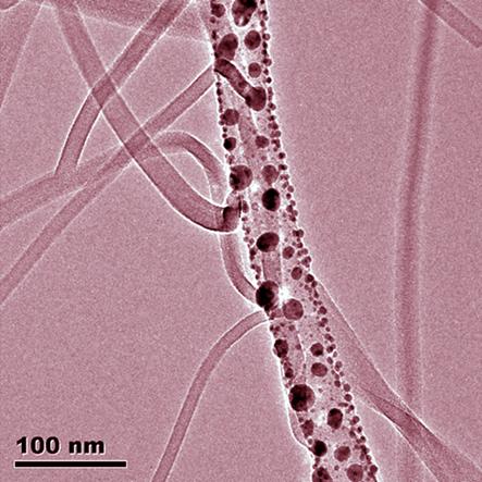
| Caption: Under the transmission electron microscope (TEM): several cobalt phthalocyanine nanowires growing out of an iron phthalocyanine nanowire which is decorated with silver particles.
| |||
| The origin: an EU project called «PHODYE» | |||
| “We were thinking in terms of a sort of electronic key for security applications, which would only react to certain optical conditions,” explains Empa physicist Pierangelo Groening. Necessary for this are transparent, strongly fluorescing thin films, so Groening and Barranco developed a plasma-deposition process in order to store fluorescing dye molecules such as metallo-proyphins, perylenes and phthalocyanines unmodified and at high concentrations in SiO2 or TiO2 layers. | |||
| It soon became apparent that if certain gas molecules deposited on dye particles in the thin films, then these fluoresced at different wavelengths and the thin film changed color as a result. If different dyes are used then the gases which are toxic to humans can be detected at very low concentrations. | |||
| A surprisingly wide range of uses | |||
| In the meantime the Empa researchers made progress, learning how to manufacture nanowires with very widely varying characteristics by appropriately selecting the starting molecule and the experimental conditions. Nanowires of metallo-phthalocyanine molecules have diameters of a mere 10 to 50 nanometers and a length of up to 100 microns. What is unusual and unexpected about the new method is that by exactly controlling the substrate temperature, molecule flow and substrate treatment, the organic nanowires develop a previously unattained, perfectly monocrystalline structure. | |||
| | |||
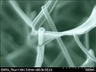
| Caption: Under the scanning electron microscope (SEM): palladium octaethyl-porphyrin nano-lamellae and nanowires growing on a perylene nanowire which has been sputtered with silver particles. | ||
| | |||
| Immediately after the first studies were made with the electron microscope it was clear to Groening that the new process could not only provide nanowires for the gas sensors but also make it possible to create complex “nanowire electric circuits” for electronic and optoelectronic applications such as solar cells, transistors and diodes. This is because the different types of nanowires can be combined as required to form networks with widely varying properties, as Groening and coworkers report in the scientific journal «Advanced Materials» and elsewhere. | |||
| The trick to achieving this lies in a second step in which the nanowires growing on the surface are “decorated” with silver nanoparticles by a sputter-coating process. A target, in this case a piece of solid silver, is bombarded with energetic ions, knocking off silver atoms which enter the gas phase and are deposited onto the nanowires. In a final step, the Empa team now grow more nanowires which, thanks to the silver particles, are in electrical contact with the original wires – the basis of an electrical circuit on the nanometer scale. | |||
| The first step from microelectronics to nanoelectronics | |||
| Take, for example, nanowires consisting of sections made with different starting molecules. If these molecules can transport either only positive or only negative charges, then a diode is created which allows current to flow in one direction alone. Groening speculates that it is quite possible that one day components for nanolectronics and nanophotonics will be made using this technique. | |||
| |||
| |||
| |||